Hi Pete,
I am trying to make the point that if an amateur amateur like me can
do it, anyone can :-)
73, Dimitris VK1SV
2013/2/5 M0FMT <[email protected]>:
> Hi Dimitrios and group
>
> Just to say thank you for publishing your transverter/converter design in
> such fine detail. It is an example to us all.
>
> 73 es GL Pete M0FMT IO91UX
>
> From: Dimitrios Tsifakis <[email protected]>
> To: [email protected]
> Sent: Tuesday, 5 February 2013, 9:28
> Subject: Re: Re: LF: My transmit converter description
>
> Hi Eike,
>
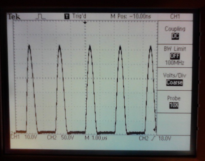
> you are right, the drain voltage waveform is not perfect! I have since
> corrected the duty cycle on the gate to be exactly 50%. I have also
> added two 200 V zener diodes from the drain to the source. This will
> clamp the voltage to 400 V which is quite safe for a 500 V FET. The
> zener diodes together with the fuses, I think, make this design pretty
> bullet proof.
>
> 73, Dimitris
>
> PS Nothing wrong with your english :-)
>
>
> 2013/2/5 Eike Katzera <[email protected]>:
>> Hi Dimitros,
>> the pulse shape in this picture does not look good:
>> http://people.physics.anu.edu.au/~dxt103/472/nltt/vk1sv-drain.jpg
>> The reason seams to be the duty cycle at the gate. Please try to change R5
>> to a 100k potentiometer and trim it to a clean single Pilse an the drain.
>> I
>> solved the same problem tha way in my PA, wich killed my IRF540.
>> Kind regards
>> Eike DL3IKE
>> PS: sorry for my english ;)
>> Gesendet: Dienstag, 05. Februar 2013 um 08:45 Uhr
>> Von: "Victor van Kooten" <[email protected]>
>> An: [email protected]
>> Betreff: Re: LF: My transmit converter description
>> Looks very nice Dimitris,hope to see/hear you soon,
>>
>> 73
>>
>> Victor
>>
>>>>> Dimitrios Tsifakis <[email protected]> 05/02/2013 01:50 >>>
>> Hello group,
>>
>> My transmit converter is now finished and tested - it survived two
>> sessions of 50% duty cycle WSPR transmissions on 475 kHz and the
>> results are great. I thought others may find this useful, so I have
>> put a write-up on my web page:
>>
>> http://people.physics.anu.edu.au/~dxt103/472/nltt/
>>
>> It is a 50 W class-e PA designed for 50 ohm impedance, so there is no
>> need for an impedance transformer. Doesn't get simpler than that :-)
>> The driving circuit is based on G3XBM Roger's design with the
>> difference of a 10 MHz OCXO LO and the addition of a beefy MOSFET
>> driver.
>>
>> 73, Dimitris VK1SV
>>
>>
>>
>>
>
>
>
|