Return to KLUBNL.PL main page

rsgb_lf_group
[Top] [All Lists]

Re: LF: Decca 5501

To: [email protected]
Subject: Re: LF: Decca 5501
From: Andy Talbot <[email protected]>
Date: Wed, 13 Jan 2016 16:08:18 +0000
Dkim-signature: v=1; a=rsa-sha256; c=relaxed/relaxed; d=gmail.com; s=20120113; h=mime-version:in-reply-to:references:date:message-id:subject:from:to :content-type; bh=68kJjOdnKlS6ZLqI32Od599jbTVGLguqPX+0ZV5E0IU=; b=ltTj+zrbsJNIMC03QJy+EUCNIHIGCwmYVKgTd3bee713fOSuK4CJCMLLq8UBlOmlwR JlFe6s2RpgG768vnvooXPZWwxMu91hPr/AcwAEve2O9GYsS0ul7RdSAv4v06MYiGlB5+ gMUllAIdj+dxe7VPrVIfGfvVU5kYnARAlNe5uhDI0xpUGMSKkpILxSdC/W4gxl9tfAbz XcOQxOe+/vewLTvOUZzcRC/XiHh5VF9E1FJ/Nrtem4vLkbr5pEXyphTDhUnEPt1RpSXw SjXI6+HPNfSO5n0KR8XCnWxyiMH5SZihNbZYdU5HHTGlr7KE+KoFQk7LRXemlRFktXGZ yj0A==
In-reply-to: <[email protected]>
References: <CAA8k23TtYRiFm8F_9EtxnApgLLHSHcLuurPm9L=mYw+viPKQiA@mail.gmail.com> <[email protected]>
Reply-to: [email protected]
Sender: [email protected]
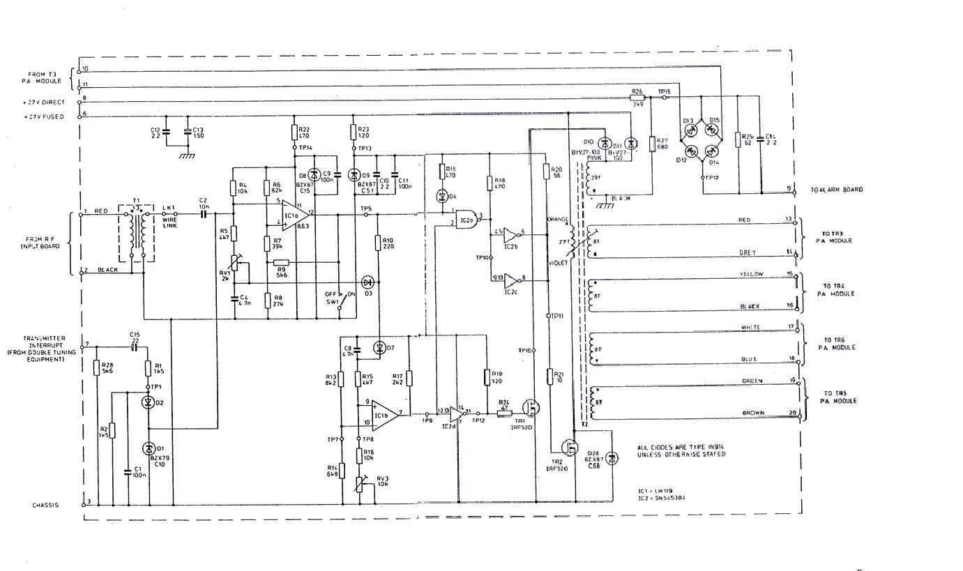
I've knitted together Fig4a  and  4b. the driver circuitry  as http://www.g4jnt.com/DownLoad/Decca5501_Driver.gif

It's not at all clear, and looks a ling winded way of doing things, but I guess that is more to do with component availability in the 1970's

The "on" drive via TR2 comes direct from the squarer IC1a and two gates
The "off" or clamp drive takes the output of the squarer, goes through a delay (R10, C8 and inexplicably D7), another opamp to square things up again and into D1.

It looks as if all that complexity is there to give some dead time between the A side on and B side on periods. That will get passed through to the output devices and prevent current spikes due to unequal switch on / off times.   In which case the various zeners and clamp diodes are there to protect the driver devices themselves from high voltage transients during the dual-off period.

Oh the joys of circuit design in that era when everything had to be done with basic components - instead of an EE lookup table or a DSP chip

Andy  G4JNT

On 13 January 2016 at 15:26, <[email protected]> wrote:
OK thanks Andy I do have the circuit diagrams but I understood that the clamp only operated if the drive was lost. The description was not that clear to me but a probe with the scope may clear that up. I have added resistors across the fet gates  so that if the transformer fails the fet should turn off. I think I was lucky when the transformer failed and the fet was not  killed! The insulation in the transformer is only what is on the litz wire and it has sleeving out of the coil. It failed as the ferrite is earthed and it had degraded the insulation over time. It was a pig to wind but was worth it, no spares are probably available unless from a scrap unit.
Dave


-----Original Message-----
From: Andy Talbot <[email protected]>
To: rsgb_lf_group <[email protected]>
Sent: Wed, 13 Jan 2016 10:45
Subject: Re: LF: Decca 5501

I've just looked again, and there's more to to the drive circuitry than that.  It is single ended drive for current into the inductor, as I stated, but there is another IRF520 used as an active clamp (the circuit diagram was drawn a bit ambiguously, so didn't spot the arrangement straightaway).  So when these two FETs are driven alternately there will be a proper equal amplitude symmetrical drive waveform generated.

It is definitely used as an energy storage inductor though, hence a gapped core is essential. 

'jnt 

On 13 January 2016 at 10:23, <[email protected]> wrote:
Andy thanks for that I am looking to find a scrap amplifier module to play around with with a view to rebuild the PCB and drive circuits. Looking on a scope the switching is very symmetrical but that may be only luck. I have used pushpull fets to drive another amp I designed and it worked well using a rewound driver transformer from a pc power supply. The complete setup is now on the QRP labs website if you want to have a look, look under GW8GLO.
73 Dave


-----Original Message-----
From: Andy Talbot <[email protected]>
To: rsgb_lf_group <[email protected]>
Sent: Wed, 13 Jan 2016 9:51
Subject: Re: LF: Decca 5501

Bit late now, but I found the circuit of the Deca transmitter on G3XDV's website. http://homepage.ntlworld.com/mike.dennison/index/lf/decca/transmitter.htm.
(Look at Fig 4, 'right' )

The driver circuit is just a single IFR520 FET switching into the transformer, so there is a net DC component - and of course it has to be a gapped core.  In fact I'm a bit surprised at that circuitry, considering it has to switch the FETs alternately on each half of the output waveform, a single ended, flyback drive like that cannot possibly be symmetrical.  Especially as the only reverse clamp appears to be a 68V zener..  But no doubt it is 'good enough'    In my 137kHz Tx design - very loosely based on the Decca output stage, I used a ferrite transformer  (ungapped)  and AC coupling from the driver IC into that.

Andy  G4JNT


On 9 January 2016 at 09:26, <[email protected]> wrote:
Thanks for the reply the transformer failed because of a small cut in the rubber sleeving where it entered the ferrite. As the ferrite is earthed the insulation on the litz was not good enough. I have a diagram and used that to help rewind the new transformer. There does not appear to be any DC component flowing in any winding according to the diagram. This unit has possibly been exposed to damp conditions as two of the input transformers were also OC primary and were rebuilt. One set of gate windings are running at the OP from the bridge and this is the one that failed. I am thinking of rebuilding the whole drive board to improve the isolation. I have already added voltage regulators to supply the ICs, this makes the 27v current a lot lower!
73 Dave


-----Original Message-----
From: Andy Talbot <[email protected]>
To: rsgb_lf_group <[email protected]>
Sent: Fri, 8 Jan 2016 18:53
Subject: Re: LF: Decca 5501

The fact it is a GAPPED core is of more significance than that of the type of ferrite.   In a transformer application - as that appears to do - it is surprising that a gapped one is used.   I do not have the circuit of the Decca transmitter to hand, but can only assume the driver has DC passing through the winding, hence the need to introduce an air gap to prevent ferrite saturation.

In which case, the fact your unit overheated suggests your gap was too small and the Vt product (volt-seconds is what saturates ferrite, not current).   BUT if that was the was the original unit, you need to ask the question why it should have failed before trying to replace it.    Those transmitter units were very reliable under rated things, so components failing need investigating.

Andy  G4JNT

On 8 January 2016 at 11:09, <[email protected]> wrote:


Does anybody know what ferrite grade is used on the fet driver transformer. I have had one burn out and have rebuilt it but would like to redesign it with better isolation between windings. Have tried various cores but cannot get the same clean waveform. The original is a gapped core of unknown material ferrite. Does anybody have a scrap amp unit that I can use for testing. The finished mods have given 1 kw at 53 volts, can be driven up to 75 volts but dummy load cannot take it!!!
73 Dave GW8GLO


<Prev in Thread] Current Thread [Next in Thread>